- Original Article
- Open access
- Published:
Subsurface Defect Evaluation of Selective-Laser-Melted Inconel 738LC Alloy Using Eddy Current Testing for Additive/Subtractive Hybrid Manufacturing
Chinese Journal of Mechanical Engineering volume 34, Article number: 111 (2021)
Abstract
New materials and manufacturing technologies require applicable non-destructive techniques for quality assurance so as to achieve better performance. This study comprehensively investigated the effect of influencing factors including excitation frequency, lift-off distance, defect depth and size, residual heat, and surface roughness on the defect EC signals of an Inconel 738LC alloy produced by selective laser melting (SLM). The experimental investigations recorded the impedance amplitude and phase angle of EC signals for each defect to explore the feasibility of detecting subsurface defects by merely analyzing these two key indicators. Overall, this study revealed preliminary qualitative and roughly quantitative relationships between influencing factors and corresponding EC signals, which provided a practical reference on how to quantitively inspect subsurface defects using eddy current testing (ECT) on SLMed parts, and also made solid progress toward on-line ECT in additive/subtractive hybrid manufacturing (ASHM) for fabricating SLMed parts with enhanced quality and better performance.
1 Introduction
Additive manufacturing (AM) technique is designed to fabricate structures using a ‘layer-by-layer’ approach as opposed to the conventional ‘bottom up’ subtractive manufacturing (SM) [1]. After extensive studies during the past three decades [2], AM has been able to offer a great deal of superior advantages for efficiently building parts with freedom of design, mass customization, waste minimization, fast prototyping as well as high geometric and material complexities [3,4,5]. These are exactly the reasons why varied AM techniques are pervasively applied in various fields spanning from aerospace, automobile industries to biomedical engineering [6]. Despite those favorable features, the current AM techniques are often confronted with multiple shortcomings, such as limitation on materials, formation of various defects, relatively poor surface finish, low dimensional and geometric accuracies, which jointly lead to the inferior mechanical properties and practical performance of AM-built parts [3]. Among the shortcomings, internal defects such as porosities, cracks and incomplete fusion holes in the produced parts play an vital role in deteriorating the overall properties [7, 8]. As a result, these shortcomings greatly hinder further application and popularization of AM techniques in industry [9].
In order to overcome the shortcomings concerning AM-produced parts, a novel manufacturing technique termed as additive/subtractive hybrid manufacturing (ASHM) has been developed by generally integrating CNC machining into an additive manufacturing system for the sake of complementing the advantages of both approaches as well as minimizing their limitations [10, 11]. Over the past decades, a large variety of efforts have been exerted on the development of various types of ASHM techniques. Manogharan et al. [12] put forward a novel approach by combining electron beam melting (EBM) with CNC machining to study how machining parameters influenced the costs associated with the AM and SM methods. Li et al. [13] proposed a novel 6-axis hybrid additive-subtractive manufacturing process using a six degrees of freedom robotic arm, which displayed a great potential in reducing material waste and production time, as well as improving the surface quality of the built parts. Du et al. [7] introduced a new strategy for ASHM of metallic parts by exploiting both simplex AM and precision milling. After a comprehensive characterization of parts manufactured by various parameters, the study summarized a valuable guide for determining the ASHM process parameters. Although the present ASHM techniques are realized through combinations of AM and SM techniques, the research put an emphasis on control of external surface quality and overall dimensional accuracies. However, the interior defects beneath a surface were still not taken into account, not to mention in-process defect detection and in-situ removal in the ASHM process. Therefore, the way of integrating defect detection and removal into the ASHM process is highly beneficial and essential in reducing interior defects and further improving the strength and fatigue life of an AMed part.
In view of this situation, for the purpose of precisely locating and characterizing internal defects without altering the original attributes or harming the examined material, numerous types of non-destructive testing (NDT) methods are extensively investigated accordingly. Among those frequently studied methods, optical inspection is able to directly detect abnormal melting pools, but the accuracy for detecting subsurface defects is generally not high enough for practical applications [14]. For directly locating subsurface defects, spatially resolved acoustic spectroscopy (SRAS) is adopted to inspect both surface and subsurface defects of the polished parts produced by selective laser melting (SLM) [15]. However, it is difficult for SRAS to detect the subsurface defects deeper than 100 μm, which substantially limits its further practical applications. For more precise and direct inspection of internal defects, X-ray computed tomography (XCT) allows effective data acquisition of internal defects, and is introduced for porosity and discontinuity detection in components made by SLM [16]. However, this technique is time-consuming in data acquisition, relatively cumbersome in configuration and hazardous to personnel from possible radiation. Therefore, it is nearly impossible to be integrated into an ASHM system. In addition, ultrasonic inspection has been considered as another promising technique in detecting subsurface defects. However, the couplant which is dedicated to transmitting the ultrasonic signals is indispensable, which makes it difficult or even impossible to be applied on complex shaped or fast-moving components [17]. Moreover, as a contact-type technique, the ultrasonic technique cannot be used at an elevated temperature above 227 ℃ which is often the case in ASHM [18]. In light of this problem, in order to get rid of the couplant, an air-coupled ultrasonic inspection is employed for defect detection, but it must be operated at frequencies less than 1 MHz with a limited spatial resolution [19,20,21]. In this way, the air-coupled ultrasonic inspection is only applicable for preliminary determinations of defect size and location [22,23,24].
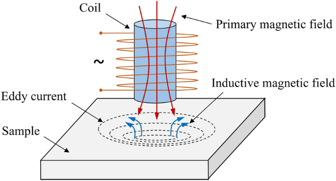
Although the NDT techniques mentioned above have their respective advantages under certain circumstances, they are generally unsuitable for ASHM. Therefore, for the purpose of circumventing the drawbacks of the NDT techniques, an effective technique called eddy current testing (ECT) is thus established accordingly because ECT can be easily applied in a large variety of materials only if the materials being tested are electrical conductors where eddy currents can flow, just as the schematic shown in Figure 1. As EC is highly sensitive to small defects in surface and subsurface layers [25], a defect can be detected and analyzed by ECT without complicated information processing. Moreover, ECT is performed in a speedy and simple procedure, which not only reduces complicity but also saves time. Most importantly, its non-contact detecting style allows for direct inspection of high-temperature samples without any couplants or coolants [26], thus rendering it fairly suitable as a quality assurance device for an AM or ASHM system [27].
Due to its superior advantages over other NDT techniques, the ECT technique has attracted more and more attention over the past few decades. Tsukada et al. [28] developed a novel ECT probe by using a dual-channel tunneling magnetoresistance sensor, which was helpful for detecting defects in steel parts even at narrow points. Mohanty et al. [29] established a correlation between defect depth and diffusion time of eddy currents through which the full sensitivity (0.5‒1 nT) of the fluxgate sensor was realized in a noisy environment. Inspired by the capability of ECT, Jain et al. [30] verified the feasibility of detecting defects in laser welded aluminum alloy packages through innovatively incorporating the GaAs-based bare monolithic microwave integrated circuits in an ECT device. As the EC signal was always interfered by the noise in the environment, Koyama et al. [31] hence proposed two novel types of probes to detect axial defects and circumferential defects, respectively. As a result, a relationship between the phase angle and depth of surface defects was established. In our previous study, for the purpose of facilitating on-line inspection and repair operations, Du et al. [32] integrated a commercial EC detector in an ASHM system. The whole manufacturing process is repeated in a loop as shown in Figure 2: material deposition (AM, Figure 2(a)) → machining (SM, Figure 2(b)) → defect detection (ECT, Figure 2(c)) → defect removal (SM, if any, Figure 2(d)) → material deposition (AM, Figure 2(f)) [32]. In the loop of ASHM, defect can occur at any time, so in-situ ECT will be performed after melting several layers of metal powders (the thickness must be less than the detection limit of ECT tester, which is usually thinner than 500 μm). Before performing ECT, the SLMed layers will be machined using the milling cutter to eliminate the interference of surface unevenness on capturing EC signals. Once internal defects are detected by the ECD tester, the depth of defects will be calculated based on the EC signals. Then the SLMed layers can be machined with the calculated depth of cut using the milling cutter. After milling, the ECD is performed again to detect the defect, if defects are detected, the defect can be removed using the milling cutter until the intensity of defect EC signal is weak than the tolerance. Thus, the SLMed layers are free of significant defects detectable by the EC detector. After that, SLM continues for several layers, milling and ECT are repeated in a loop as mentioned above.
There are some prerequisites for the application of ASHM. In ASHM, the parameters and process for SLM are supposed to be highly mature and optimized, and the SLMed parts should to be highly dense and stable. Therefore, ECT is used for quality assurance not for instructing parameter optimization, which means ECT is mainly used to detect several possible significant defects in dense bulk material that may be induced because of sudden power fluctuation of laser beam or occasional instability of powder melting. Due to the limit of ECT tester, current ECT cannot detect too small defects smaller than 200 μm, but current experimental results [7, 32] verify that it’s feasible to detect significant defects and ensure that the SLMed layers are free of significant defects detectable by the EC detector. Therefore, current ECT tester is qualified to act as quality assurance of SLMed parts when only significant defects may appear. Thus, it doesn’t matter when the ECT tester doesn’t have the ability to detect defects smaller than 200 μm.
In the study, SLM is employed as one of the AM techniques to prepare the sample, i.e., Inconel 738LC alloy. Inconel 738LC alloy is a low carbon nickel-based superalloy which is strengthened mainly through the precipitation of γ′ phase (Ni3(Al, Ti)) and L12 crystal structure [33, 34]. Owing to its favorable features, such as high temperature strength, toughness, hardness, oxidation resistance and wear resistance [35], Inconel 738LC alloy has been widely utilized as structural materials in aviation [36, 37], space, chemical, and petrochemical industries, etc. [38]. To the best of authors’ knowledge, the majority of the previous studies pertaining to defect inspection with ECT mostly focus on materials produced by the conventional manufacturing methods, few nickel-based superalloys (including Inconel 738LC alloy) have been processed by SLM at present, not to mention to test the SLMed Inconel 738LC alloy by using ECT. In addition, conventional ECT requires multiple defect EC signals and complicated signal processing to obtain useful information of subsurface defects. Therefore, in this study, the authors quantitatively investigated the effects of excitation frequency, lift-off distance (the distance between probe and sample surface), depth of defect (the distance between the vertex of defect and the probe), residual heat, defect size and surface roughness on the detected EC signals of the SLMed Inconel 738LC alloy sample. As two key indicators, both the impedance amplitude and phase angle of EC signals for each defect were simultaneously recorded and analyzed to investigate how they varied with the detection parameters, so as to explore the feasibility of revealing the information of subsurface defects by merely analyzing these two key detection indicators of defect signals.
2 Experimental Methods
2.1 Sample Preparation
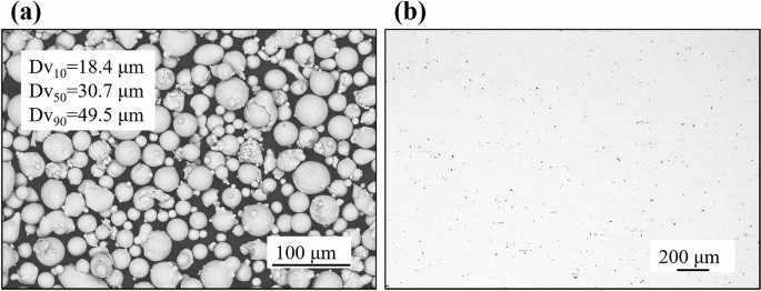
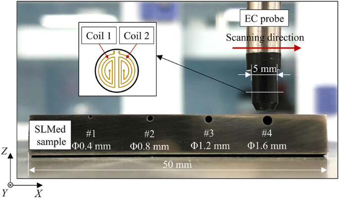
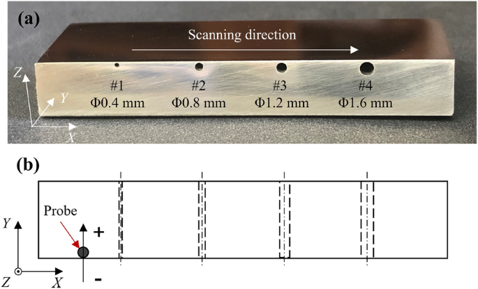
Commercial Inconel 738LC powders with an average particle size of 30.7 μm (as displayed in Figure 3(a)) were used to additively manufacture a bulk alloy sample with dimensions of 50 mm×10 mm×15 mm on an SLM machine (SLM Solutions 125HL, Germany). In Figure 3(a), Dv10, Dv50 and Dv90 respectively mean that 10%, 50%, and 90% of the total particles are smaller than this size. The average chemical compositions of the Inconel 738LC powders are listed in Table 1. The mass density of the SLMed bulk Inconel 738LC alloy sample was tested to be higher than 99 %, only micro defects (average defect size < 20 μm) randomly scattering in a sample as shown in Figure 3(b). After the SLM process, an SLMed Inconel 738LC alloy sample was machined by sinker electric discharge machining (SEDM) and the machined sample is illustrated in Figure 4. The sample is featured with four through holes (cylindrical defects) with the diameter of 0.4 mm, 0.8 mm, 1.2 mm and 1.6 mm, respectively, as well as two parallel oblique planes with a 10° inclination angle with respect to the cylindrical defects. Although the artificial defect sizes are generally larger than the existing defects in the SLMed sample, it’s useful to study the correlations between each influencing factor including excitation frequency, lift-off distance, defect depth and size, residual heat, and surface roughness, and corresponding EC signals.
2.2 Setup for Eddy Current Testing
As shown in Figure 5, a differential EC probe with a diameter of 5 mm is adopted in this study. The differential EC probe consists of two coils wound in opposite direction, which is capable of effectively detecting the magnetic field change induced by the defect at a high sensitivity. When one of them locates above a defect, a difference in inductance is induced between these two coils, which reflects the features of the defect such as depth, size or shape etc. It is also able to suppress the noise interference and detect smaller defects during an AM process [39].
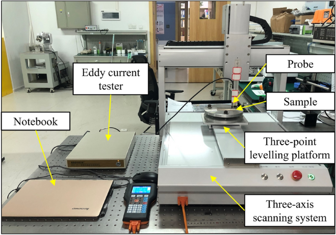
The ECT setup (displayed in Figure 6) mainly consists of five major components, i.e., a three-axis scanning system, a three-point levelling platform, a computer, an EC tester and a probe connected up with the EC tester. The probe of the EC tester is mounted on the three-axis scanning system with which the probe is able to travel at a speed from 1 to 1000 mm/s with a positioning accuracy of 0.01 mm, and the travel range of the three-axis scanning system is 500 mm along the three axes, i.e., X, Y and Z axis. The three-point levelling platform placed on the three-axis scanning system is dedicated to keep the upper surface of sample parallel to the travel direction of the probe. Besides that, the computer connected up with the commercial EC tester (EDDYSUN EEC 35++, China) is installed with a dedicated software for the purpose of adjusting the parameters of excitation signals and analyzing the data captured by the probe.
2.3 Mechanism of Eddy Current Testing
ECT works on the principle of Faraday’s law. It detects variations in coil impedance in the same exciter coil or voltage change in a separate coil [40]. When the exciter coil is placed on different materials, the coil impedance or voltage change in the receiver coil varies due to the changes in electrical resistivity and magnetic permeability of the materials [41]. The schematic representation of the test coils is shown in Figure 5. The eddy current principle can be explained by the following electromagnetic equations [42]:
where Z is the magnitude and Φ is the phase angle of impedance. R is the resistance and ωL is the inductive reactance of the circuit.
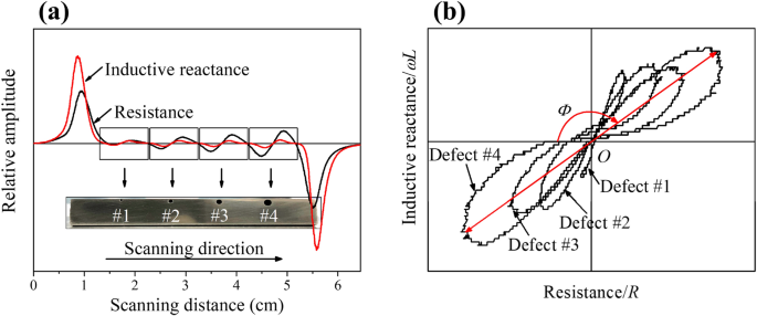
Figure 7 shows the typical defect EC signals around the defect location along the scanning direction and the corresponding loops on the impedance plane, respectively. For each testing, a defect EC signal can be divided into two components, i.e., resistance and inductive reactance which vary with the location of the probe while scanning, as shown in Figure 7(a). Figure 7(b) displays the corresponding loops on the impedance plane. The included angle between the inclination direction of each curve and the negative direction of horizontal axis (resistance) is defined as phase angle, annotated as angle Φ in the figure [43]. Phase angle is a relatively independent indicator regardless of the defect size and surface roughness [31], if the depth of defect with different sizes is kept constant, the defect phase remains almost the same. In addition, the defect phase angle is less impacted by surface roughness [43], which indicates that effective ECT for internal defects can be conducted even on a rough surface only if signal-to-noise ratio (SNR) is well suppressed and the effective defect EC signals can be extracted. In this regard, the phase angle can be adopted as a key indicator to reflect the depth of defect in ECT as well as for further application in ASHM. Therefore, the amplitude and phase angle of the loop obtained by the dedicated software are used to analyze the effect of influencing factors in ECT.
2.4 Experimental Procedures of ECT
Table 2 summarizes the testing parameters adopted in this study for achieving a good SNR. For all ECT tests, the signal gain and scanning speed were kept consistent and fixed at 35 dB and 600 mm/min, respectively; and the eddy current scanning was conducted in the impedance sweep mode where the impedance plane represented by resistance and inductive reactance could be obtained. In order to eliminate background interference, every time prior to inspecting defect signals, the EC signals captured from the defect-free section of the sample were set to zero by automatically adjusting the output offset.
In the ECT experiments, the first step was to determine the optimal frequency for detecting the four artificial defects. As shown in Figure 8(b), the black circle denoted the location of the probe in the Y direction equal to zero, i.e., Y = 0. The probe scanned along the longitudinal direction (X axis), and the excitation frequency was adjusted from 30 to 1000 kHz to investigate how the amplitude of EC signals shifted accordingly, while the lift-off distance was constantly fixed at 0.07 mm. In order to investigate the influence of the lift-off distance and depth of defect, two different detecting strategies were introduced to the experiment. The first strategy was implemented in this way: fixing the location of the probe in the Y axis at zero (Y = 0), and scanning in the X axis by using the optimal excitation frequency acquired from the previous step, then increasing the lift-off distance and scanning again, just repeating the route by this means and gradually elevating the height of the probe starting from the minimum 0.07 mm to 1.60 mm. The other strategy was also carried out in a scanning-moving-scanning manner as described in the first strategy, the only difference laid in that: after each scanning the probe moved 0.20 mm towards the positive Y direction from a starting location at Y = − 3 mm, then the probe scanned again, while maintaining the lift-off distance fixed at 0.07 mm in the process.
Another influencing factor that needs to be taken into account is the temperature involved in the process of SLM and SM because it can cause considerable errors to the EC probe. If the probe is kept in close contact with a testing part with high temperature, the heat radiated from the sample may not only damage the probe but also cause an undesired impedance change in the probe, thus impeding the defect detection [44]. In this regard, non-contact inspections are considered as the simplest and most convenient method to attenuate this effect [44]. However, by keeping the probe away from the sample material, the magnetic induction inside the sample material declines sharply, causing it more difficult to detect defects due to the reduced EC signals [44]. Therefore, it is necessary to study the influence of temperature on defect detection. In order to investigate the effect of temperature on defect EC signals, a heating plate was utilized to heat up the sample to simulate the temperature environment in the SLM process. In the experiment, the location of the probe in the Y axis was kept constant at Y = 0, the optimal excitation frequency was kept consistent with that obtained in the previous tests, the lift-off distance of the probe was fixed at 0.2 mm so as to avoid probe damage from the hot heating plate.
The last factor to consider is surface roughness of the bulk Inconel 738LC alloy sample. In the process of ASHM, SM (e.g., milling) always follows AM before ECT is conducted, so the surface discontinuity and unevenness caused by SM will more or less introduce noise to the detected EC signals, thus reducing SNR in ECT. Given this situation, it is strongly necessary to assess the influence of surface roughness on the EC signals to exclude the impact of roughness introduced by SM in ECT. In light of this, four types of abrasive papers with mesh sizes of #80, #180, #1000 and #2000 were used to polish the upper surface near the four defects (as shown in Figure 5). Each time after polishing with one type of the abrasive papers, a digital microscope (VHX-7000, Keyence, Japan) was utilized to examine the surface morphology and measure the surface roughness of the sample.
In this study, for each influencing factor, both the impedance amplitude and phase angle of corresponding EC signals for each artificial defect were simultaneously recorded. In addition, triple estimates were used to obtain the quantitative values, and the results are presented as arithmetic means plus standard deviations.
3 Results and Discussion
3.1 Effect of Excitation Frequency
In ECT, there are two crucial influencing factors, i.e., eddy current density and penetration depth, dominating the selection of excitation frequency for subsurface defect detection. Penetration depth determines how deep the probe can inspect for subsurface defects in ECT, which depends on the electrical conductivity and magnetic permeability of the testing material as well as the EC excitation frequency exerted on the material. The penetration depth can be calculated as Eq. (4) [45,46,47], which can also be converted as Eq. (5):
where δ is the standard penetration depth in m, σ is the electrical conductivity in S/m, μ is the magnetic permeability in H/m, ω is the angular velocity defined by ω = 2πf, and f is the excitation frequency in Hz [47]. For a given material, the electrical conductivity and magnetic permeability of the material is normally considered to be constant, so excitation frequency is the only key factor affecting the penetration depth. According to Eq. (5), the penetration depth is inversely proportional to the square root of the excitation frequency, indicating that a lower frequency is more preferred for improving the penetration depth of EC.
However, the absolute eddy current density is a function of the magnetic field strength and the excitation frequency which are intensively influenced by the penetration depth [46]. As penetration depth is getting larger, the corresponding eddy current density attenuates exponentially on account of the skin effect which refers to the phenomenon that occurs when the frequency of the excitation signal is increased, eddy current is thus induced to a thin layer (or skin layer) near the surface of a sample [32, 39, 48]. Based on the above mentioned, boosting excitation frequency brings about two consequences. The first is that a higher frequency reduces the penetration depth of EC according to Eq. (5), the second is that a smaller penetration depth leads to higher eddy current density due to the skin effect. In general, an increase in excitation frequency causes two opposite effects in the ECT of subsurface defects. Therefore, it is a vital issue to balance between these two contradictory effects for the purpose of identifying a suitable excitation frequency in a successful ECT of subsurface defects.
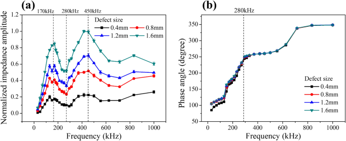
In this study, the optimal excitation frequency is determined in terms of the normalized amplitude of the defect EC signals calculated from the impedance plane. As illustrated in Figure 9(a), the normalized impedance amplitudes of the four defect EC signals are positively correlated with the defect sizes, and all the curves fluctuate with an increase in the excitation frequency. It is worth noticing that every curve features with two peaks, which is ascribed to the competitive effect of the boosted excitation frequency. As the frequency increased, the curves soared up from the beginning and reached a peak at near 170 kHz. During the process, the influence caused by EC penetration depth played a major role. As the frequency was further improved, the curves continued to drop to a valley around 280 kHz, then soared up thereafter until arrived at another peak at about 450 kHz. During this period, the penetration depth slowly decreased, reflecting that less defect EC signal was captured. When the amplitude of the curves approached another peak at about 450 kHz, the impact generated from skin effect played a dominant role. Similar to that occurring in decreasing penetration depth, the eddy current density near the subsurface of the sample became higher with boosting frequency because of the skin effect. After the frequency surpassed 450 kHz, the curves dropped off gradually due to the weakening effect of those two factors on the amplitude of the defect EC signals.
As shown in Figure 9(b), the corresponding impedance phase angles of the EC signals from the four defects increase with frequency. There is also a turning point at around 280 kHz where the four curves are clearly divided into two stages. In the first stage, with an increase in the frequency from the beginning to around 280 kHz, a sudden increase appeared around 170 kHz, and the difference among the four curves gradually decreased. However, in the second stage after frequency surpassing 280 kHz, four curves almost overlapped completely. Interestingly, the phenomenon displayed in Figure 9(b) properly verified that observed in Figure 9(a). In the first stage, the influence resulted from the EC penetration depth played a leading role, so the phase angles varied among different defect sizes. However, in the second stage, the excitation frequency was so high that the dominant skin effect caused high-density eddy current concentrating at almost the same depth, hence the four curves of the defect EC signals detected from the same depth superposed accordingly.
Because of the skin effect, the high-frequency eddy current tends to concentrate in the surface layer of a material with its amplitude attenuating more drastically than that with the lower frequency. As a result, in order to suppress the skin effect, lower frequency, e.g., 170 kHz, was more preferred for detecting defects with ECT in the SLMed Inconel 738LC alloy sample. Hence, 170 kHz was utilized as the excitation frequency in the subsequent experimental investigations.
3.2 Effect of Lift-off Distance and Residual Heat in ECT
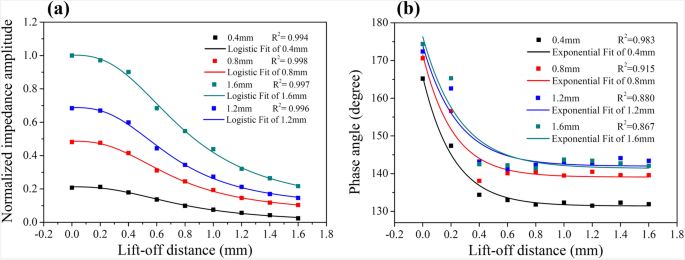
As a critical geometric factor in ECT, the lift-off distance is considered as an undesirable noise source and normally exerts a negative impact on the amplitude of defect EC signals [32] which can be summarized as follows: the higher the lift-off distance, the weaker the inductive defect EC signals [49]. Figure 10(a) and (b) demonstrate the normalized impedance amplitude and impedance phase angle of the EC signals from the four defects in regard to the lift-off distance, respectively. As displayed in Figure 10(a), during the course of elevating the lift-off distance from 0.07 to 1.60 mm, the impedance amplitude of the defect signal was positively proportional to defect size, and the four curves all revealed a gradually descending trend. When the lift-off distance was increased to 1.60 mm, the impedance amplitude of the EC signal from defect #1 became too weak to distinguish. The equation that best fits these points in Figure 10(a) is a logistic function given by Eq. (6), where A1, A2, x0, and p are constants:
The values of these constants as well as the correlation coefficient (R2) of fitting curves are given in Table 3. Four fitting curves all yield a correlation coefficient of over 0.99, which indicates highly reliable fitting results by using the logistic function.
However, the impedance phase angle in Figure 10(b) displays a totally different trend with increasing lift-off distance. As the probe was lifted to 0.4 mm from 0.07 mm, the phase angle of the four curves drastically dropped by about 30°. Then, the curves remained almost level thereafter. The phenomena revealed in Figure 10(a) and (b) can be interpreted as follows. With elevating the lift-off distance, the amplitude of the defect EC signals sharply attenuated accordingly but all four defects were detected in the process. It indicated that for each defect the effect of lift-off distance worked in the variation of phase angle before the lift-off distance reaching 0.4 mm. However, the phase angles of the EC signals were kept constant after the lift-off distance reaching 0.4 mm, indicating that the defect EC signals were captured from the same depth and the lift-off distance exerted no significant impact in the meanwhile. An exponential equation as shown in Eq. (7) is used to fit these points in Figure 10(b), where A, y0, and R0 are constants.
The values of these constants as well as the correlation coefficient of fitting curves are given in Table 4. The exponential equation properly describes the variation of phase angle with increasing the lift-off distance for four groups of data.
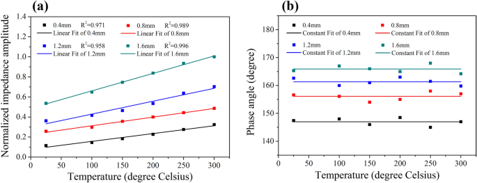
In practical applications, ECT has to be conducted at a certain lift-off distance so as to protect the probe from physical or thermal damage. This is because in the ASHM of Inconel 738LC alloy, temperature on the contact surface may rapidly rise due to intensive heat release in the laser fabrication and machining process, so residual heat still remains after completing the manufacturing process [50]. In light of these considerations, the sample was heated up from 25 to 300 °C in the experiment to simulate the temperature conditions. As displayed in Figure 11(a), EC signals are sensitive to temperature change. By raising the temperature, the normalized magnitude of the defect EC signals illustrates a near-linear increase, which can be ascribed to the reduced magnetic permeability and electric conductivity of the Inconel 738LC alloy due to increased vibrations of the crystal lattice that impede the motion of the conduction electrons [39, 51]. A linear equation is employed to fit the data in Figure 11(a), and the high correlation coefficients of over 0.95 confirm the reliability of linear fitting. The boosting EC signal amplitude in this situation can be interpreted in this way: as other parameters were fixed except the temperature, the penetration depth went deeper with the reduced magnetic permeability and electrical conductivity of the material caused by higher temperature according to Eqs. (4) and (5) [51], thus defect EC signals with a greater magnitude were captured as shown in Figure 11(a). However, unlike the variation of the amplitude of EC signals, the phase angles are kept stable with increasing the temperature, as shown in Figure 11(b). As other parameters except temperature are kept constant, it indicates that the phase angles are irrelevant to the temperature of the sample. In addition, the change of phase angle in Figure 11(b) is the same as that revealed in Figure 10(b), which also implies that the phase angle of the defect EC signals varies with the defect size. As a result, the findings revealed in Figure 11(a) and (b) indicate that non-contact ECT can be performed on an Inconel 738LC alloy sample with temperature as high as 300 ℃ while keeping a safe lift-off distance. In terms of incorporating ECT on an ASHM machine, although the temperature has an impact on detection accuracy of ECT, the results indicate that the impact is fairly limited.
3.3 Effect of Defect Depth
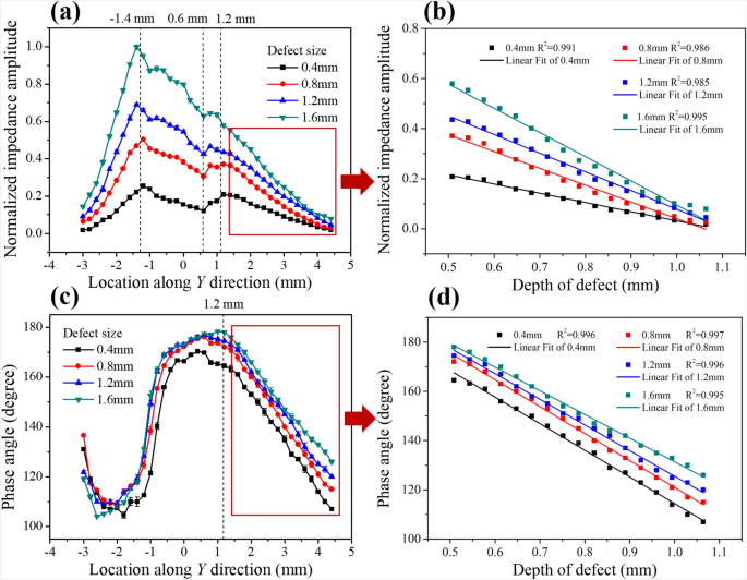
In the ECT of Inconel 738LC alloy sample, the detection depth for subsurface defects is another crucial influencing factor to assess the potential of integrating the ECT equipment into an ASHM machine. Figure 12(a) and (c) reveal the effect of the depth of defect on the normalized impedance amplitude and phase angle of the EC signals from four defects along the Y direction. In the experimental investigation, the probe started at Y = − 3 mm, and gradually moved towards the positive Y direction. The origin of the Y axis (Y = 0) was denoted by a black circle as illustrated in Figure 8(b). As shown in Figure 12(a), the signal amplitude of the four curves all demonstrate a positive correlation with defect size, which monotonically increase to a maximum value from Y = − 3.0 mm to Y = − 1.4 mm along the Y axis. Then the curves take on a descending trend to a minimum value at Y = 0.6 mm. At last, after a small rise at Y = 1.2 mm the curves decline until where it is difficult to distinguish among the four curves. Figure 12(b) illustrates the magnified part in Figure 12(a) and converts the horizontal axis from Y positions to the corresponding depth of defects. These four linear fitting curves indicate a perfect inversely proportional relationship between impedance amplitude of defect signals and the depth of defect.
In terms of the phase angle, as the probe moved along the Y axis, the four curves arrived at a minimum value at location Y = −2 mm at first then reached a peak at Y = 0.6 mm, generally illustrating drastic fluctuation around the origin point of the Y axis, as shown in Figure 12(c). Figure 12(d) illustrates the magnified part in Figure 12(c) after Y exceeding 1.2 mm and converts the horizontal axis from Y positions to the corresponding depth of defects. It’s worth noticing that the phase angle and the depth of defect also illustrates a linear relationship. In theory, with the probe moving along the Y axis, the amplitude of a defect EC signal should firstly increase then decrease steadily without any anomalies, because the amplitude is negatively correlated with the depth of defect in this circumstance and there ought to be only one minimal depth of defect. Thus, there exists only one maximal amplitude around the origin point in the Y axis where the depth of the defect is the lowest. However, in the present experiment, the amplitude anomalies of defect EC signals can be found in Figure 12(a), the corresponding phase angles also fluctuate wildly, as shown in Figure 12(c). As a result, the findings in Figure 12(a) and (c) indicate that as the periphery reflects the EC signal and impedes its propagation, the defect EC signals were significantly affected by the periphery of a sample, thus bringing about signal anomalies as illustrated in Figure 12(a) and (c). Moreover, it is also interestingly to notice that the curves of amplitude and phase angle all take on a monotonically descending trend without any fluctuations after location Y = 1.2 mm, which suggests that they should be less influenced by the periphery and could be used as indicators to reflect the relationship between the defect EC signals and the depth of defect.
3.4 Effect of Surface Roughness
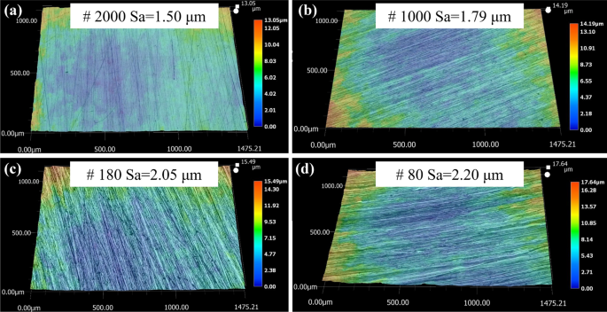
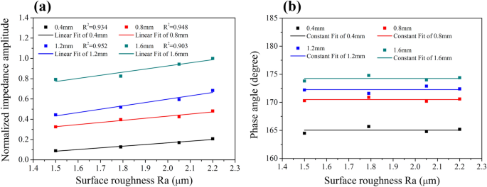
In the process of AM, rapid melting and solidification of melt pools inevitably introduce surface discontinuity and unevenness to a sample, acting as numerous micro-defects, which will more or less affect the accuracy and reliability of ECT. As shown in Figure 13, it includes the surface 3D profiles and the values of surface roughness (Sa) of the sample after grinding with various types of abrasive papers. It reveals that the surface roughness of a sample is positively proportional to the roughness of abrasive papers. As shown in Figure 14, the corresponding amplitude and phase angle of the EC signals from the four defects reveal the same trend as displayed in Figure 11. A linear equation is employed to fit the data in Figure 14(a), and the high correlation coefficient of over 0.90 confirms the reliability of linear fitting. For each defect, the amplitude of the EC signals declined with increasing surface roughness, while its phase angle remained constant in the process. Since prior to inspecting defect signals, the EC signals captured from the defect-free section of the sample were set to zero by automatically adjusting the output offset so as to eliminate background interference, therefore, the surface with large roughness produced more noises, which thereby caused a greater loss to the amplitude of the defect EC signals after eliminating the background interference. In addition, a coarser surface means greater surface discontinuity, which, in a certain extent, alters the properties of the sample surface thus affecting the defect EC signals. In terms of the phase angle, it keeps stable while increasing the surface roughness, which indicates that the phase angle of EC signals is nearly not affected by the surface roughness of the sample.
3.5 Effect of Defect Size
In SLMed parts, there normally exists three types of defects, i.e., spherical porosities, incomplete fusion holes, and cracks [8, 52]. The size of different defects varies in a large range from 10 μm [53] to over 200 μm [54], and a qualified sample prepared by SLM normally does not contain defects with a size over 100 μm. In this study, in order to detect the defect size as well as evaluate the performance of ECT on the SLMed Inconel 738LC alloy sample, four artificial defects with a minimal size 0.4 mm were machined by SEDM due to its machining size limit. The testing sample had a high mass density of > 99 %, only containing a few defects as small as 20 μm as illustrated in Figure 3(b). The size of the small defects was far beyond the detection limit of the ECT tester, thus nearly exerting no influence on the defect EC signals. Although the artificial defect sizes are generally larger than the existing pores in the SLMed sample, this study is mainly aimed to investigate the correlations between defect sizes and corresponding EC signals, further study is still needed to improve the detecting accuracy of subsurface defects in SLMed parts.
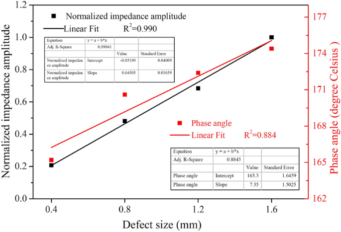
The experiment conducted in this study uncovered preliminary qualitative and roughly quantitative correlations between the EC signal and the defect size, as shown in Figures 9(a), 10(a), 11(a), 12(a) and 14(a), the amplitude of the EC signals increases with an increase in defect size, implying that the EC signal amplitude generally shows a positive correlation to defect size no matter how other parameters may change, which is in good accordance with that reported by Du et al. [32]. For roughly quantifying the relationship between defect size and the impedance amplitude of defect signals, linear fit curves are adopted as shown in Figure 15, and yield relatively high correlation coefficients. In this regard, the amplitude of an EC signal is a feasible indicator representing the size of subsurface defect in the SLMed parts.
In terms of the relationship between the defect size and the phase angle of the corresponding defect EC signals, there is a similar trend between the amplitude of the EC signals and the defect sizes, i.e., larger defects generate defect EC signals with higher phase angles, as shown in Figures 10(b), 11(b), 12(c) and 14(b). As displayed in Figure 15, linear fit curves are used to roughly quantify the relationship between defect size and the corresponding phase angle of defect signals. Although the phase angle of an EC signal is proportional to the defect size, the correlation is not as strict as that revealed between the amplitude of EC signals and the defect sizes, for example in Figure 9(b). More in-depth quantitative investigations based on physical models are still needed in future research to establish precise correlations between the geometrical features of defects and various influencing factors in ECT.
4 Conclusions
This study evaluates the applicability of ECT technique in detecting subsurface defects in an SLMed Inconel 738LC alloy sample. After a comprehensive investigation on the effects of excitation frequency, lift-off distance, defect depth and size, residual heat, and surface roughness, on the defecting EC signals from the Inconel 738LC alloy sample produced by SLM, preliminary qualitative and roughly quantitative relationships between these influencing factors and the amplitude and phase angle of the corresponding defect EC signals are revealed as summarized in the following.
-
(1)
The variation of amplitude and phase angle of defect EC signals are governed by logistic and exponential equations respectively with increasing the lift-off distance.
-
(2)
Non-contact ECT is applicable to detecting defects at an elevated temperature up to 300 ℃, and the phase angle of defect EC signals is nearly not affected by the temperature.
-
(3)
EC tests are strongly affected by the edge effect, which however can be weakened if the probe doesn’t move across the edge. The amplitude and phase angle of defect EC signals are both revealed to be negatively proportional to the depth of defect when testing away from the edge.
-
(4)
Surface roughness introduces more noises to the detection signal and compromises the amplitude of defect EC signals, but nearly exerts no influence on the phase angle of defect EC signals.
-
(5)
The amplitude and phase angle of defect EC signals are both revealed to be positively proportional to the defect size, and can be taken as feasible indicators representing the size of subsurface defects.
In general, this study reveals preliminary qualitative and roughly quantitative relationships between each influencing factor including excitation frequency, lift-off distance, defect depth and size, residual heat, and surface roughness, and corresponding EC signals based on a sample with artificial defects, which achieves solid progress. Despite the fact that ASHM isn’t mature enough to detect too small or too deep defects, nor differentiate the types of internal defects in SLMed parts, it doesn’t prevent current ASHM technique from removing significant defects within 1 mm depth beneath the surface with a milling cutter under the instruction of the ECD tester.
In future works, more comprehensive considerations on the interplay among these influencing factors in the real cases of SLMed parts will be intensively investigated, and more efforts need to be exerted on improving the accuracy for detecting smaller defects with a size less than 200 μm even 100 μm, so as to improve the detecting efficiency and accuracy of ASHM. In addition, further works still remain on the development of integrated control software, prototyping of ECT systems, and process optimization of ECT for the advancement of ASHM.
References
A Zocca, P Colombo, C M Gomes, et al. Additive manufacturing of ceramics: Issues, potentialities, and opportunities. Journal of the American Ceramic Society, 2015, 98(7): 1983-2001.
M K Thompson, G Moroni, T Vaneker, et al. Design for additive manufacturing: Trends, opportunities, considerations, and constraints. CIRP Annals, 2016, 65(2): 737-760.
T D Ngo, A Kashani, G Imbalzano, et al. Additive manufacturing (3D printing): A review of materials, methods, applications and challenges. Composites Part B: Engineering, 2018, 143: 172-196.
S A M Tofail, E P Koumoulos, A Bandyopadhyay, et al. Additive manufacturing: Scientific and technological challenges, market uptake and opportunities. Materials Today, 2018, 21(1): 22-37.
S Singh, S Ramakrishna, R Singh. Material issues in additive manufacturing: A review. Journal of Manufacturing Processes, 2017, 25: 185-200.
N Guo, M C Leu. Additive manufacturing: technology, applications and research needs. Frontiers of Mechanical Engineering, 2013, 8(3): 215-243.
W Du, Q Bai, B Zhang. A novel method for additive/subtractive hybrid manufacturing of metallic parts. Procedia Manufacturing, 2016, 5: 1018-1030.
B Zhang, Y Li, Q Bai. Defect formation mechanisms in selective laser melting: A review. Chinese Journal of Mechanical Engineering, 2017, 30(3): 515-527.
J Delgado, J Ciurana, C A Rodríguez. Influence of process parameters on part quality and mechanical properties for DMLS and SLM with iron-based materials. The International Journal of Advanced Manufacturing Technology, 2012, 60(5): 601-610.
W Du, Q Bai, B Zhang. Machining characteristics of 18Ni-300 steel in additive/subtractive hybrid manufacturing. The International Journal of Advanced Manufacturing Technology, 2017, 95(5-8): 2509-2519.
B Lauwers, F Klocke, A Klink, et al. Hybrid processes in manufacturing. CIRP Annals, 2014, 63(2): 561-583.
G Manogharan, R A Wysk, O L A Harrysson. Additive manufacturing–integrated hybrid manufacturing and subtractive processes: economic model and analysis. International Journal of Computer Integrated Manufacturing, 2016, 29(5): 473-488.
L Li, A Haghighi, Y Yang. A novel 6-axis hybrid additive-subtractive manufacturing process: Design and case studies. Journal of Manufacturing Processes, 2018, 33: 150-160.
J A Kanko, A P Sibley, J M Fraser. In situ morphology-based defect detection of selective laser melting through inline coherent imaging. Journal of Materials Processing Technology, 2016, 231: 488-500.
R J Smith, M Hirsch, R Patel, et al. Spatially resolved acoustic spectroscopy for selective laser melting. Journal of Materials Processing Technology, 2016, 236: 93-102.
G Ziółkowski, E Chlebus, P Szymczyk, et al. Application of X-ray CT method for discontinuity and porosity detection in 316L stainless steel parts produced with SLM technology. Archives of Civil and Mechanical Engineering, 2014, 14(4): 608-614.
D Yi, C Pei, T Liu, et al. Inspection of cracks with focused angle beam laser ultrasonic wave. Applied Acoustics, 2019, 145: 1-6.
K Nadimpalli, H Gu, D Pal, et al. High frequency ultrasonic non destructive evaluation of additively manufactured components. 24th International SFF Symposium - An Additive Manufacturing Conference, 2013: 311-325.
R Kažys, A Demčenko, E Žukauskas, et al. Air-coupled ultrasonic investigation of multi-layered composite materials. Ultrasonics, 2006, 44: 819-822.
L Ambrozinski, B Piwakowski, T Stepinski, et al. Application of air-coupled ultrasonic transducers for damage assessment of composite panels. 6th European Workshop on Structural Health Monitoring, Dresden, Tyskland, 2012.
L Ambrozinski, B Piwakowski, T Stepinski, et al. Pitch-catch air-coupled ultrasonic technique for detection of barely visible impact damages in composite laminates. EWSHM - 7th European Workshop on Structural Health Monitoring, Nantes, France, 2014.
V Giurgiutiu. Embedded non-destructive evaluation for structural health monitoring, damage detection, and failure prevention. The Shock and Vibration Digest, 2005, 37(2): 505-511.
C T Ng, M Veidt. A Lamb-wave-based technique for damage detection in composite laminates. J. Smart Materials Structures, 2009, 18(18): 074006.
I Yang, K Im, U Heo, et al. Ultrasonic approach of rayleigh pitch-catch contact ultrasound waves on CFRP laminated composites. J. Mater. Sci. Technol., 2008, 24.
F Yu, M P Blodgett, P B Nagy. Eddy current assessment of near-surface residual stress in shot-peened inhomogeneous nickel-base superalloys. Journal of Nondestructive Evaluation, 2006, 25(1): 16-27.
J Garcia-Martin, J Gomez-Gil, E Vazquez-Sanchez. Non-destructive techniques based on eddy current testing. Sensors (Basel), 2011, 11(3): 2525-65.
C B Scruby. Some applications of laser ultrasound. Ultrasonics, 1989, 27(4): 195-209.
K Tsukada, M Hayashi, Y Nakamura, et al. Small eddy current testing sensor probe using a tunneling magnetoresistance sensor to detect cracks in steel structures. IEEE Transactions on Magnetics, 2018, 54(11): 1-5.
I Mohanty, R Nagendran, A V Thanikai Arasu, et al. Correlation of defect depth with diffusion time of eddy currents for the defects in conducting materials using transient eddy current NDE. Measurement Science and Technology, 2018, 29(10): 105601.
A Jain, N V Sheth, C N Lal. Inspection of laser welded hermitically sealed packages using eddy current flaw detection method. 2015 International Conference on Computer, Communication and Control (IC4), 2015: 1-5.
K Koyama, H Hoshikawa. Eddy current flaw testing probe with high performance in detecting flaws during in-service inspection of tubing. Electrical Engineering in Japan, 2007, 161(2): 52-61.
W Du, Q Bai, Y Wang, et al. Eddy current detection of subsurface defects for additive/subtractive hybrid manufacturing. The International Journal of Advanced Manufacturing Technology, 2017, 95(9-12): 3185-3195.
P Wangyao, P Jariyasakuntham, S Polsilapa, et al. Effects of Al additions and reheat treatments on microstructures of modified nickel-based superalloy, grade inconel 738, by vacuum arc melting process. Advanced Materials Research, 2014, 1025-1026: 395-402.
E Balikci, A Raman, R A Mirshams. Tensile strengthening in theNi-base superalloy IN-738LC. Journal of Materials Engineering and Performance, 2000, 9(3): 324-329.
K Kunze, T Etter, J Grässlin, et al. Texture, anisotropy in microstructure and mechanical properties of IN738LC alloy processed by selective laser melting (SLM). Materials Science and Engineering: A, 2015, 620: 213-222.
Z Mazur, A Luna-Ramírez, J A Juárez-Islas, et al. Failure analysis of a gas turbine blade made of Inconel 738LC alloy. Engineering Failure Analysis, 2005, 12(3): 474-486.
O A Ojo, N L Richards, M C Chaturvedi. Liquid film migration of constitutionally liquated γ′ in weld heat affected zone (HAZ) of Inconel 738LC superalloy. Scripta Materialia, 2004, 51(2): 141-146.
L Li, J Dong, M Zhang, et al. Integrated simulation of the forging process for GH4738 alloy turbine disk and its application. Acta Metallurgica Sinica, 2014, 50(7): 821-831.
N Bowler. Eddy-current nondestructive evaluation. Springer-Verlag New York, 2019.
A Nusair Khan, S H Khan, F Ali, et al. Evaluation of ZrO2–24MgO ceramic coating by eddy current method. Computational Materials Science, 2009, 44(3): 1007-1012.
M H Nateq, S Kahrobaee, M K Torbati. Nondestructive characterization of induction hardened cast iron parts. 2nd International Conference on Materials Heat Treatment, 2011.
P Xu, S Huang, W Zhao. A new differential eddy current testing sensor used for detecting crack extension direction. NDT & E International, 2011, 44(4): 339-343.
V M A Silva, C G Camerini, J M Pardal, et al. Eddy current characterization of cold-worked AISI 321 stainless steel. Journal of Materials Research and Technology, 2018, 7(3): 395-401.
J B Bento, A Lopez, I Pires, et al. Non-destructive testing for wire + arc additive manufacturing of aluminium parts. Additive Manufacturing, 2019, 29.
H M G Ramos, O Postolache, F C Alegria, et al. Using the skin effect to estimate cracks depths in mettalic structures. 2009 IEEE Intrumentation and Measurement Technology Conference, 2009: 1361-1366.
G Mook, O Hesse, V Uchanin. Deep penetrating eddy currents and probes. Materials Testing, 2006, 48(5): 258-264.
S Bajracharya, E Sasaki, H Tamura. Numerical study on corrosion profile estimation of a corroded steel plate using eddy current. Structure and Infrastructure Engineering, 2019, 15(9): 1151-1164.
R Nagendran, N Thirumurugan, N Chinnasamy, et al. Optimum eddy current excitation frequency for subsurface defect detection in SQUID based non-destructive evaluation. NDT & E International, 2010, 43(8): 713-717.
A Christophe, Y Le Bihan, F Rapetti. A mortar element approach on overlapping non-nested grids: Application to eddy current non-destructive testing. Applied Mathematics and Computation, 2015, 267: 71-82.
Z Luo, Y Zhao. Numerical simulation of part-level temperature fields during selective laser melting of stainless steel 316L. The International Journal of Advanced Manufacturing Technology, 2019, 104(5-8): 1615-1635.
G Vertesy, T Uchimoto, I Tomas, et al. Temperature dependence of magnetic descriptors of magnetic adaptive testing. IEEE Transactions on Magnetics, 2010, 46(2): 509-512.
T DebRoy, H L Wei, J S Zuback, et al. Additive manufacturing of metallic components – Process, structure and properties. Progress in Materials Science, 2018, 92: 112-224.
J Elmer, J Vaja, H Carlton. The effect of reduced pressure on laser keyhole weld porosity and weld geometry in commercially pure titanium and nickel. Welding Journal, 2016, 95: 419-430.
N T Aboulkhair, N M Everitt, I Ashcroft, et al. Reducing porosity in AlSi10Mg parts processed by selective laser melting. Additive Manufacturing, 2014, 1-4: 77-86.
Acknowledgements
Not applicable.
Funding
Supported by Basic Research Project of Science and Technology Plan of Shenzhen (Grant No. JCYJ20170817111811303).
Author information
Authors and Affiliations
Contributions
BZ and SG were in charge of the whole trial; SG wrote the manuscript; GR assisted with sampling and laboratory analyses. All authors read and approved the final manuscript.
Authors’ Information
Sai Guo, born in 1993, now is a PhD candidate at Southern University of Science and Technology, China. His research interests focus on high-speed grinding and additive manufacturing.
Guanhui Ren, is a research assistant at Southern University of Science and Technology, China. His research interest is additive/subtractive hybrid manufacturing.
Bi Zhang, is currently a chair professor at Southern University of Science and Technology, China. His research interests include precision machining and additive/subtractive hybrid manufacturing.
Corresponding author
Ethics declarations
Competing Interests
The authors declare no competing financial interests.
Rights and permissions
Open Access This article is licensed under a Creative Commons Attribution 4.0 International License, which permits use, sharing, adaptation, distribution and reproduction in any medium or format, as long as you give appropriate credit to the original author(s) and the source, provide a link to the Creative Commons licence, and indicate if changes were made. The images or other third party material in this article are included in the article's Creative Commons licence, unless indicated otherwise in a credit line to the material. If material is not included in the article's Creative Commons licence and your intended use is not permitted by statutory regulation or exceeds the permitted use, you will need to obtain permission directly from the copyright holder. To view a copy of this licence, visit http://creativecommons.org/licenses/by/4.0/.
About this article
Cite this article
Guo, S., Ren, G. & Zhang, B. Subsurface Defect Evaluation of Selective-Laser-Melted Inconel 738LC Alloy Using Eddy Current Testing for Additive/Subtractive Hybrid Manufacturing. Chin. J. Mech. Eng. 34, 111 (2021). https://doi.org/10.1186/s10033-021-00633-9
Received:
Revised:
Accepted:
Published:
DOI: https://doi.org/10.1186/s10033-021-00633-9
